FPGA Based Design
Almost all of the board level designs completed by Design Interface include one or more FPGA devices. FPGAs allow complex systems comprising of millions of gates to be implemented within a few square inches of PCB area. Amongst the benefits delivered by FPGA technology are:
 High system speed
- Improved reliability
- Low power consumption
- Low electromagnetic emissions - keep the fast signals on-chip
- Reconfigurability - useful for debug, product updates and resource sharing
- Macros and IP blocks available for many functions
- Lower system cost
- On chip memory blocks, clock handling, multipliers, processors and flexible I/O
- High speed serial I/O transceivers
- Built in support for common interfaces such as PCIe, DDR3, Ethernet etc.
FPGA component pricing is no longer a deterrent for many cost sensitive systems and with the availability of on chip memory and processor macros the SoC (System on Chip) paradigm is becoming applicable to more and more designs. At Design Interface we have built up a useful library of proven functions that can be dropped straight into new designs, or as is more often the case, customised to best suit the application. For instance our synchronous DRAM controller block has formed the basis of several versions, some tuned for random cache line access, others for long bursts such as streaming data. Currently most of our FPGA development and test benches are VHDL based as is the norm in Europe.
FPGA Based Development Board
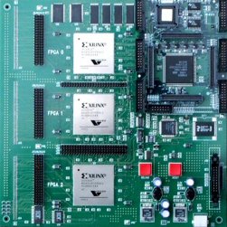
A European company developing an ARM based product ordered this board design to allow them to verify their multiple sourced schematic / VHDL / Verilog design before committing to an ASIC. A discrete ARM processor is mounted on the mezzanine board in the top right corner, the AMBA bus and other signals are connected to the FPGAs. An additional benefit was being able to supply working systems to their software developers months before the ASIC design was finalised. The fully functional prototypes allowed new features to be evaluated simply by reloading the FPGAs, thereby enhancing the utility of the final ASIC implementation.
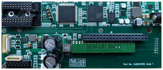
FPGA Based Controller Board I
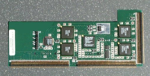
Our client for this design has kindly allowed us to publish a picture of this board, but has requested that we don't divulge its function or application. Briefly, the centrally mounted FPGA controls the other ICs on the board and several other modules attached via the board edge connectors. Data flows through the system at a sustained transfer rate of 1.44 GB/s.
FPGA Based Controller Board II
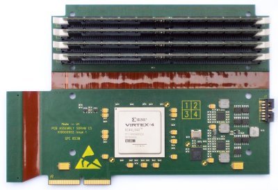
All of the functions required for this design, apart from the power supplies and DDR2 SDRAM based memory, are implemented in the FPGA. The flex-rigid PCB folds at the two hinges so that the DIMMS hang down in front of the FPGA and fit into the limited space available for this unit. A high density connector hidden behind the left most section of PCB passes fifty two high speed source synchronous differential pairs which deliver data to the FPGA, these must be independently synchronised and FIFO buffered before being stored in the memory. Simultaneously data must be fetched from the memory and delivered to the output port. The storage data rate exceeds 5 GB/s.
The product for which this board is a core component has won a Queen's Award for innovation and the innovation category in Business Weekly magazine's Business Awards 2007.
FPGA Based Controller Board III
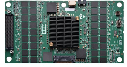
This is the most recent design in this series of high speed data storage and manipulation boards. Up to 72 GB of DDR3 memory is mounted directly on both sides of the PCB in order to minimise the required headroom. 84 gigabit links continuously deliver data at an aggregate rate in excess of 10 GB/s, processed data is simultaneously available at the output port.
FPGA Based Printer
This FPGA based motherboard supports a credit card size PC and OLED display (not shown) to implement a high speed industrial printer able to print text and graphics at 600 dpi at line speeds of 5 m/s.
Design Interface's FPGA experience stretches back to Xilinx's original XC20xx series of devices. That first FPGA based design implemented an interface between the Q-bus on a DEC Micro-VAX and a multiprocessor applications accelerator. The learning process since then has been continuous as FPGA densities and features have multiplied. Whilst synthesis, placement and routing tools are improving rapidly, an understanding of the internal structure of the devices is still a vital prerequisite in achieving the highest packing density and the highest system frequencies.


Design Interface is a Xilinx Alliance member and a Xilinx XPERTS partner.